
Electron beam lithography is used to draw a custom pattern on the surface of a material coated with a layer of resist. Upon exposure to electrons, this material either becomes highly soluble, allowing its removal by immersion in a solvent, or cross-links, making it resistant to a solvent so that the surrounding resist is removed.
Tiny nanostructures can be manufactured by electron beam lithography with high reliability and accuracy, without the need for a photomask, and at a resolution of less than 10 nm.
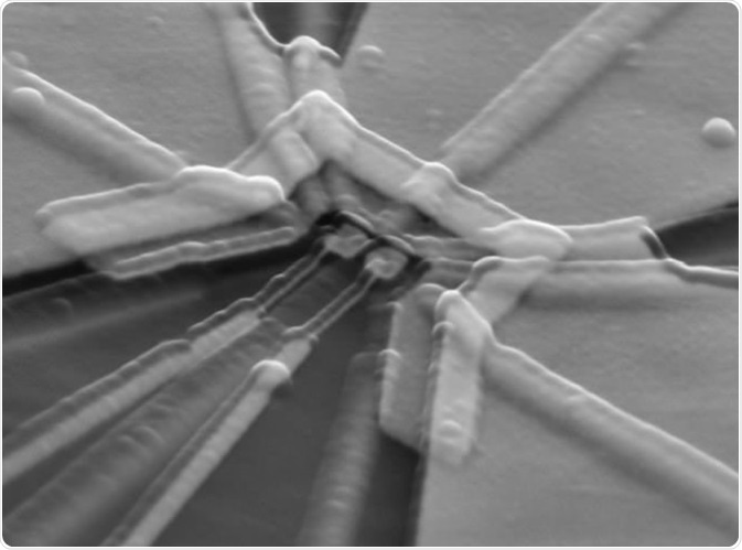
Electron Beam Lithography Process
Comparison with other methods
Electron beam lithography is slower than photolithography, stamping, or self-assembly methods that are also used in patterning. It is often more expensive and requires clean room facilities. Electron beam lithography is therefore more suited to create extremely high-resolution patterns, or unique items for which the creation of a photomask is too time consuming or wasteful.
Electron source
Hot W/ZrO2 is often used as an electron source through field electron emission, and either electrostatic or magnetic lenses is used to focus the beam. The configuration of the resist layer creates complex trough shapes, such as T-shape or stepped.
Multiple layers of resist with differing sensitivities to the electron beam induces the layers to adjust their solubility over a greater or lesser volume from the direct path of the electron beam. This is achieved through scattering, diffusion, or secondary electron production.
Grounding
During electron beam lithography, materials are exposed to an intense beam of electrons and so must be grounded electrically to avoid charging effects. Grounding is often achieved by adding a thin metal layer, often aluminium or gold, either between the substrate and resist or on top of the resist.
Electron Beam Lithography in Biology
Patterning biomolecules
Biomolecules can be patterned on a substrate surface using electron beam lithography, with the ability to create repeating structural features with different chemistries suitable for immobilizing different biomolecules in two or three dimensions. This can be done by locally adjusting the hydrophobicity of the resist, allowing biomolecules to be immobilized by hydrophobic interaction or coupling chemistries.
The surface of a gold substrate can be exposed, which can serve as self-assembled monolayer sites for various molecules. This provides a diverse range of surface chemistries to bind biomolecules which can also be made reconfigurable by using biomolecules with reversible bonding reactions.
PEG as resistant layer
Polyethylene glycol (PEG) is commonly used as a terminal thiol functional group that can form a strong covalent Au-S bond with gold, while the opposite terminal end of the molecule can be functionalized in a number of ways.
PEG also provides a protein resistant layer to the gold, ensuring that no unintended biomolecules adhere to the surface. PEG can be directly grafted onto a substrate using a dilute aqueous PEG solution and electron beam induced cross-linking, without using a resist layer.
Cells can be cultured on such a substrate, preferentially adhering to unexposed regions, and being confined by the surrounding PEG or resist layers.
Sources
- Electron-Beam Lithography for Patterning Biomolecules at the Micron and Nanometer Scale – https://pubs.acs.org/doi/10.1021/cm202669f
- Nanofabrication by electron beam lithography and its applications: A review – https://www.sciencedirect.com/science/article/pii/S016793171500101X
- E-beam lithography for micro-∕nanofabrication – https://www.ncbi.nlm.nih.gov/pmc/articles/PMC2917861/
Further Reading
- All Lithography Content
- What is Focused Ion Beam Lithography?
- Photolithography Microfabrication Technique
Last Updated: Oct 28, 2018

Written by
Michael Greenwood
Michael graduated from Manchester Metropolitan University with a B.Sc. in Chemistry in 2014, where he majored in organic, inorganic, physical and analytical chemistry. He is currently completing a Ph.D. on the design and production of gold nanoparticles able to act as multimodal anticancer agents, being both drug delivery platforms and radiation dose enhancers.
Source: Read Full Article